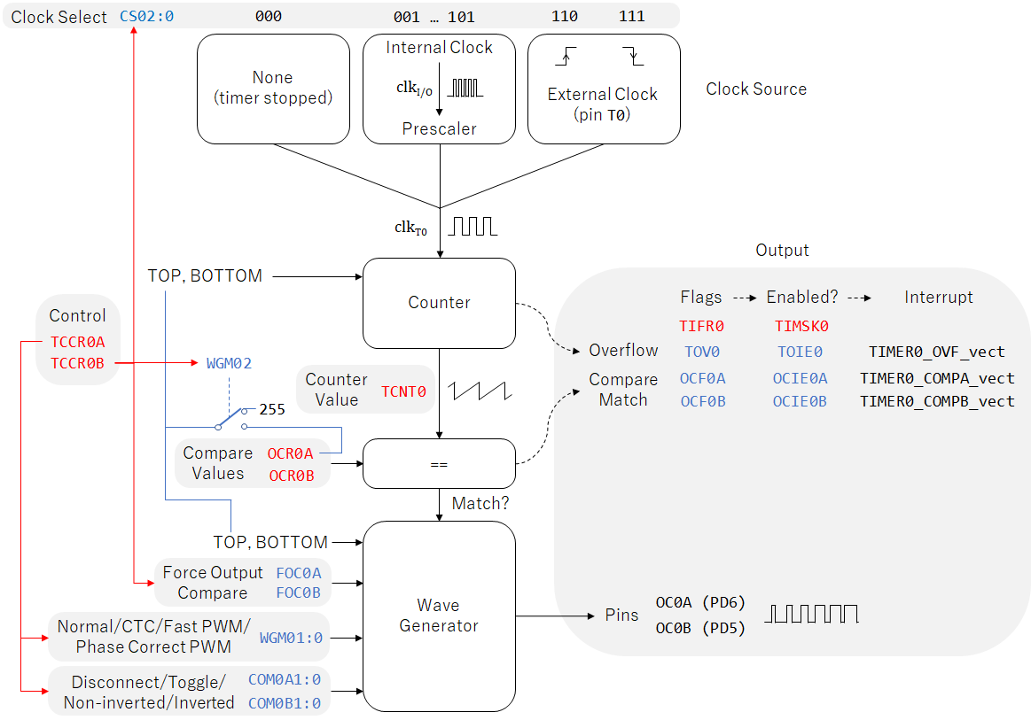
Timer/Counter0
Below is sample code to set up Timer/Counter0 on ATmega328P.
#include <avr/io.h>        // For TIMER0_OVF_vect, PRR, TCCR0A, etc.
#include <avr/sfr_defs.h>  // For _BV().
#include <avr/interrupt.h> // For sei(), ISR().
#include <avr/power.h>     // For power_timer0_enable().

ISR(TIMER0_OVF_vect)
{
	...
}

// Set compare output mode
TCCR0A &= ~(_BV(COM0A0)); // OC0A disconnected
TCCR0A &= ~(_BV(COM0A1));
TCCR0A &= ~(_BV(COM0B0)); // OC0B clear on match
TCCR0A |=   _BV(COM0B1);

// Clear OC0B pin (PD5)
TCCR0B |= _BV(FOC0B); // Write 1 to force output compare

// Set PD5 pin as output.
DDRD |= _BV(DDD5);

// Set waveform generation mode
// Compare output mode is now clear-on-match, set-at-BOTTOM
TCCR0A |= _BV(WGM00); // Fast PWM
TCCR0A |= _BV(WGM01);
TCCR0B |= _BV(WGM02); // TOP = OCR0A

// Initialize counter and output compare values
TCNT0 = 0;
OCR0A = 100; // Set PWM frequency (TOP)
OCR0B = 25;  // Set PWM duty cycle

// Clear interrupt flags to prevent interrupt
// subroutines from being called immediately after
// enabling interrupts (Note: write 1 to clear).
TIFR0 |= _BV(TOV0);  // Overflow
TIFR0 |= _BV(OCF0A); // Output compare match A
TIFR0 |= _BV(OCF0B); // Output compare match B

// Set interrupt enable bits
TIMSK0 |= _BV(TOIE0);  // Overflow enabled
TIMSK0 |= _BV(OCIE0A); // Output compare match A enabled
TIMSK0 |= _BV(OCIE0B); // Output compare match B enabled

// Set global interrupt enable bit (initially disabled)
sei();

// Enable Timer/Counter0 module
// PRR &= ~(_BV(PRTIM0)); // Write 0 to enable
power_timer0_enable(); // Same as above line

// Set clock select (start counting)
TCCR0B |=   _BV(CS00); // 1/64 prescaler
TCCR0B |=   _BV(CS01);
TCCR0B &= ~(_BV(CS02));
Register Summary
Below are all 7 registers related to Timer/Counter0.
| Registers |
Bits |
|
Control
(Settings) |
TCCR0A |
COM0A1:0, COM0B1:0 |
Compare output mode |
WGM01, WGM00 |
Waveform generation mode |
TCCR0B |
WGM02 |
CS02:0 |
Clock select |
FOC0A, FOC0B |
Write 1 to force output compare |
| Counter |
TCNT0 |
|
|
Output
Compare |
OCR0A |
|
|
OCR0B |
|
|
| Interrupt Flag |
TIFR0 |
TOV0 |
Overflow |
OCF0A, OCF0B |
Output compare match |
Interrupt Mask
(Enable Bits) |
TIMSK0 |
TOIE0 |
Overflow |
OCIE0A, OCIE0B |
Output compare match |
In addition to above, there is PRTIM0 bit in
PRR register which controls power reduction settings
of Timer/Counter0 module.
All 8 registers above have initial value 0x00.
Writing to TCNT0 blocks all compare matches
for one timer clock cycle. If TCNT0 equals
OCR0A/OCR0B,
compare match will be missed.
Power Reduction
PRTIM0 (Power Reduction Timer/Counter0) is a read/write bit
in PRR (Power Reduction Register).
It must be 0 to use Timer/Counter0. Writing 0 enables Timer/Counter0 module.
| Timer/Counter0 |
PRTIM0 |
Enabled (operating)
(initial value) |
0 |
| Disabled (shut down) |
1 |
Clock Select
|
|
Register: TCCR0B |
|
|
CS02 |
CS01 |
CS00 |
| Timer/Counter stopped (initial value) |
0 |
0 |
0 |
Internal clock source
(internal oscillator or
external crystal on pins
XTAL1 and XTAL2) |
No prescaling |
0 |
0 |
1 |
| 1/8 prescaling |
0 |
1 |
0 |
| 1/64 prescaling |
0 |
1 |
1 |
| 1/256 prescaling |
1 |
0 |
0 |
| 1/1024 prescaling |
1 |
0 |
1 |
External clock source on pin T0 |
Clock on falling edge |
1 |
1 |
0 |
| Clock on rising edge |
1 |
1 |
1 |
For example, Arduino UNO uses 1/64 prescaling with 16MHz crystal so
TCNT0 increments every 4µs (0.25MHz).
Waveform Generation Mode
|
TOP |
WGM02 |
WGM01 |
WGM00 |
Normal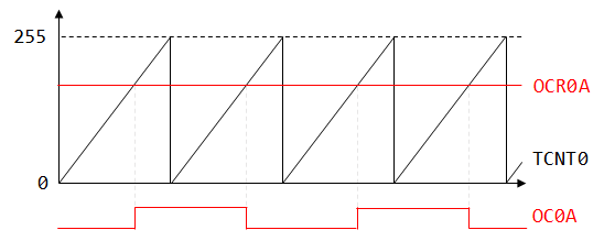 (initial value) (initial value) |
0xFF |
0 |
0 |
0 |
CTC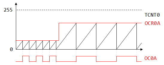 |
OCR0A |
0 |
1 |
0 |
Fast PWM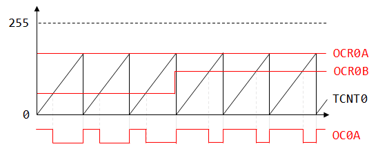
OCR0A/OCR0B updates at BOTTOM |
0xFF |
0 |
1 |
1 |
OCR0A |
1 |
1 |
1 |
Phase Correct PWM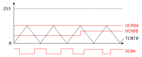
OCR0A/OCR0B updates at TOP |
0xFF |
0 |
0 |
1 |
OCR0A |
1 |
0 |
1 |
- Only
WGM02 bit is in a different register.
- Adjust frequency by varying TOP.
Compare Output Mode
Override GPIO with waveform generator on pins
OC0A/OC0B (PD6/PD5):
Step 1: Set or clear OC0A/OC0B.
These are internal bits (initially 0) that directly translate to
pin outputs only if COM0A1:0/COM0B1:0
bits are set and pins are configured as outputs.
In normal and CTC modes, writing 1 to
OCF0A/OCF0B bits
updates OC0A/OC0B as if a real match had occured.
OC0A/OC0B keep their values even when changing
between waveform generation modes.
Therefore, force match in normal mode to set or clear
OC0A/OC0B and then change waveform mode.
Step 2: Set port to output.
Write 1 to DDD6/DDD5
bits in DDRD to set pins as outputs.
These bits are initially 0 (inputs).
Pin OC0A (PD6)
|
|
|
Register: TCCR0A |
| Normal/CTC |
Fast PWM |
Phase Correct PWM |
COM0A1 |
COM0A0 |
| Disconnected (initial value) |
0 |
0 |
| Toggle |
Toggle* |
0 |
1 |
| Clear |
Clear
(set at BOTTOM) |
Up-counting: clear
Down-counting: set |
1 |
0 |
| Set |
Set
(clear at BOTTOM) |
Up-counting: set
Down-counting: clear |
1 |
1 |
*Only valid when WGM02 is 1.
Pin OC0B (PD5)
|
|
|
Register: TCCR0A |
| Normal/CTC |
Fast PWM |
Phase Correct PWM |
COM0B1 |
COM0B0 |
| Disconnected (initial value) |
0 |
0 |
| Clear |
Clear (set at BOTTOM) |
Up-counting: clear
Down-counting: set |
1 |
0 |
| Set |
Set (clear at BOTTOM) |
Up-counting: set
Down-counting: clear |
1 |
1 |
Interrupt
- Interrupt Flag
- Hardware sets to 1 at overflow/compare match
- Hardware sets to 0 when entering interrupt function
- Write 1 to clear
- Interrupt Enable Bit
- 1 = enabled
- 0 = disabled (initial value)
Appendix